|
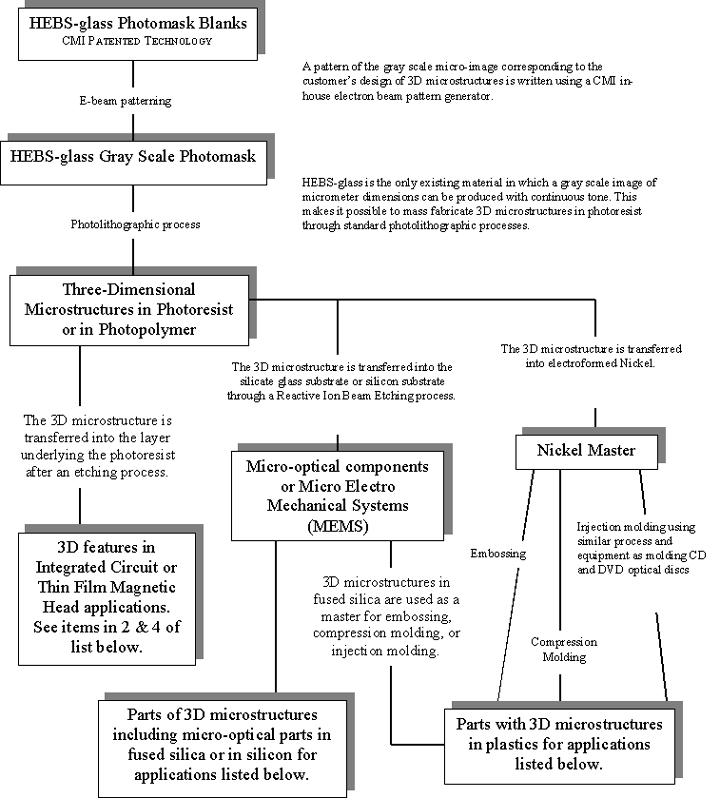
Fabrication Process & Applications of HEBS Glass Mask Technology
Surfaces with 3D microstructures are required in several fields of microtechnologies.
Many of these microtechnologies have been staged primarily in research
laboratories of universities and national laboratories in the past twenty
years, because there has been no economical means to mass fabricate these
microstructures with high precision.
HEBS-glass mask technology allows for the fabrication of master masks
that will enable the manufacturing of completely arbitrary surface profiles
using semiconductor fabrication processes. This means that any imaginable
optical requirement that can be designed can be built using HEBS-glass
gray scale mask technology.
Listed below are just a few of the potential new and existing applications:
 Micro-optics:
-
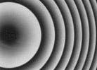
Diffractive optical elements (DOE)
-
Micro-mirror arrays and micro-prism arrays
-
Surface relief height standards and slope standards
-
Micro-splitter array for color separation (i.e. to replace the color filter
array of LCD’s)
-
Lenslet arrays including refractive micro-lens array and diffractive micro-lens
array
-
Diode laser couplers
-
Diffraction gratings, fan-out gratings
-
Beam shaping and homogenizing
-
Aberration compensation
-
Holographic optical elements (HOE), computer generated holograms (CGH)
-
CD players: objective lens of laser head
-
DVD players: glass HOE, plastic HOE, micro-prism, 3 beam tracking
-
Bar code scanners
-
Adaptive optics
-
Fill-factor enhancement
-
Optical interconnects
-
Beam multiplexing
Integrated circuits: via masks for sloped vias to improve step coverage
in multilayer metallization, and V-shaped grooves for dielectric isolation
in high voltage applications.
Magnetic disk drives: read write heads, sliders.
Micro-electro-mechanical (MEM) devices: sensors and actuators in
automotive, machine tools, robotics, and medical instrumentation, also
devices for applications in micro valves, inertial microsensors, micromachine
RF switches, GPS component miniaturization.
Fiber optics telecommunications: two dimensional fan-out gratings,
optical interconnect, signal switching, fiber pigtailing, and DOE to couple
light from a laser into a fiber.
Micro-opto-electro-mechanical (MOEM) devices: laser scanners, optical
shutters, dynamic micro-mirrors, optical choppers and optical switches.
Hybrid circuits: binary masks required for contact printing
of large number of prints without damage to the glass mask or pattern and
with tight tolerance of line width. This application utilizes in
particular the following properties of HEBS-Glass masks: (1) the mechanical
and chemical durability of an all-glass mask with an image inside the glass
(without chrome or any coating), (2) electron beam direct write mask without
any post-exposure processing steps, line width is reproducible from plate
to plate to better than 0.1 micron, because there are no resist developing
and chrome etching steps.
|