     |
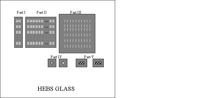
The mask pattern is written with an e-beam writer with a 0.1 mm addressing grid size and consists of the following five parts.
Part I: Part I consists of tapered structures of variable heights for applications such as micro-prisms and micro-mirrors, each facet may have a unique compound tilt. The first column (00) are prisms with a constant delta OD and the second column (01) are prisms with a constant delta T between adjacent gray levels. Each 100µm x 100µm prism has 50 gray levels. The formula for the transmittance values of the 50 graylevels in each of 20 prisms of column A is Ti = Tmax-[(Tmax-Tmin)/49]*i, where i = 0, 1, 2, 3, 4…,49. The formula for the OD values of the 50 graylevels in each of 20 prisms of column B is Odi = ODmin + [(ODmax - ODmin)/49]*i, where i = 0, 1, 2, 3, 4,…,49. The OD ranges and the corresponding transmittance ranges for the prisms in both column A and B are as follows:
Part II: This part helps users to match photoresist heights with specific optical densities (OD, or D herein after) in the mask to build a calibration curve "height of photoresist after development vs. OD of mask pattern." Part I exhibits 200 gray levels that are identified with labels, ranging from 00 to 199. Each gray level consists of one test patch, each test patch being 100µm x 100µm in size. The gray level i has an optical density value according to the equation D = 0.126 + 0.0069045226i, where i = 0, 1, 2 . . . 199. Thus, by using the equation, the minimum and maximum OD value of 200 patches can be determined to be 0.126 and 1.5, respectively. In general, the heights of resist thickness remaining will level off at an OD value between 0.8 to 1.2, because of the limited dynamic range of an analog photoresist. (Please see the CMI info sheet, "Photoresist Analog Transfer Scheme for HEBS-Glass Photomasks".) Because most photoresists have a limited dynamic range and respond to about 1 unit of OD value--for example, from 0.12 to 1.12, HEBS-Glass Plate HEBS5 with an e-beam sensitized glass layer of 1 micrometer is designed to satisfy this OD range. HEBS-Glass masks with a larger OD range can be useful for other applications such as for use with certain photopolymers and other photoresists. HEBS-Glass Calibration Plate I85 B provides test patterns and test strips having OD values up to 2.0. HEBS-Glass Plates I85 having an e-beam sensitized glass layer of 3 micron is capable of OD values up to 4.0 using an e-beam accelerating voltage of 30KV or higher. Although there are only 200 OD levels in the calibration patches, mask patterns having more than 1000 gray levels can be written in a HEBS-Glass Plate reproducibly. Any arbitrary value of OD in the OD range of 0.126 to 1.5 can be produced in HEBS-Glass Plate S5N to a precision of +/- 0.001. Namely, OD values available are D = 0.126 + 0.001i where i = 0, 1, 2, 3, ... , 1374. There exists no universal calibration curve that is valid for all users. Height of photoresist after development may be a linear or a monotonic nonlinear function of transmittance of a mask pattern, or maybe a linear or a monotonic nonlinear function of OD of a mask pattern. The variable parameters governing the calibration curve include the variable parameters of photolithography tools such as exposure wavelength and intensity, and the variable parameters of photoresists and development including the type of photoresist and the as-coated thickness of photoresist. Nevertheless, when as coated photoresist thickness is very thin such as less than 1 micrometer, it is likely that the height of photoresist after development is a linear function of the transmittance (T here in after) of the mask pattern. Part III: The test pattern of Part III represents a wider range of tapered structures and is composed of a 9x9 array of via structures that are 800 microns in length, see Diagram 1. This test pattern has nine optical density ranges that are listed in Table I. There are 20 gray levels within each of the nine optical density ranges. Table II lists these 9 sets of 20 gray levels. The 20 OD values in each of the nine ranges vary in intervals of constant delta T (first 4 rows) or constant delta OD (last 5 rows). The OD range is consistent across a row, whereas the width and gap of the via structure is consistent down a column. Table III displays the dimensions of the via structures within each column. Diagram 2 defines the via gap and via width. With this portion, together with Part II of the calibration plate, HEBS-glass users can determine the optical density (OD) range of a gray scale mask that is most appropriate for a particular device fabricated with existing in-house processes and equipment of photolithography and plasma etching. HEBS glass enables users to custom design prism gratings and v-groove spacers to achieve wavelength division multiplexing and for accurate alignment and positioning optical fibers. Other tapered structures are used in applications such as read-write heads for magnetic disk drives.
Part IV: This part contains two examples of refractive lens or beam shaper. OD values are arbitrarily increasing/decreasing. The first contains a 1 mm diameter positive lens-like OD profile. The second is 1 mm negative lens-like profile. Each is surrounded by a 1 mm frame. Part V: This part contains positive and negative refractive microlens arrays. The OD values for the arrays are arbitrarily increasing/decreasing. Each array contains 3 rows of 17 lenses; each lenslet is 50µm x 50 µm. A frame surrounds each array. Instructions for viewing mask patterns under an optical microscope: Please view mask patterns in the HEBS-glass under a microscope in a transmission mode (i.e. using the bottom light); the mask pattern has little or no contrast in a reflection mode (i.e. using the top light) because the reflectance of HEBS-glass is about 4% in both clear and e-beam darkened areas. Instructions for handling and storage: Since the mask pattern is inside the glass, HEBS-glass masks can be washed like a quartz glass substrate, using any solvent or acid (except HF). Strong base solution may cause pits in the surface of HEBS-Glass or any silicate glass. HEBS-Glass masks should be kept at room temperature. Humidity levels from 0 to 100% do not affect HEBS-glass masks.
|
| Company | Technology | Products | Online Help | Contact |