Cost Efficient Mass Fabrication of Diffractive Optical Elements (DOEs)
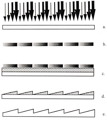
HEBS-glass is a mask material sensitive towards e-beam exposure, and the exposure with a certain electron beam dosage changes the optical density of the material. After e-beam exposure, the mask needs no further development or fixation process. The mask with multi levels of optical densities can then be used to expose a photo resist in a contact aligner or in a reduction stepper. This allows to associate a certain resist thickness after development with each optical density. The information was used to determine the e-beam dosages for each of the phase levels necessary to generate a DOE. The so generated HEBS-glass gray level mask can be used to expose numerous DOE's using an optical lithography tool. After many copies of the mask on the photo resist are developed, many substrates with the developed photo resist are placed in a CAIBE system, to simultaneously transfer the microstructures from the analog resists on the surfaces of the substrates. An overview of these processing steps is shown in Fig. 10.
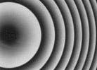
Fig. 11(a) shows an optical micrograph of a gray level mask. The DOE array shown in Fig. 11(b) was generated using HEBS-glass gray level mask of Fig. 11(a) and the processing techniques exhibited in Fig. 10. This scanning electron micrograph shows an array of 10 by 10 spherical on axis lenses, the aperture size of the lenses is 50x50 microns and the lenses are designed for use with 830nm wavelength.
The described fabrication method shows the cost effective mass fabrication of DOEs. There are a number of advantages:
The mass fabrication is simplified and more cost-effective. Instead of a set of masks (i.e. 5 masks for 32 phase levels) with all the associated resist processing, only a single mask needs to be exposed in the e-beam writer and no resist processing is associated with the mask generation.
All phase levels are written in a single step on a single mask. The inevitable miss registrations and associated efficiency losses between subsequent exposures are avoided.
Third, the number of processing steps for the DOE fabrication compared to binary mask fabrication of 32 phase levels is reduced by a factor of 5. This will reduce the cost for high quality monolithic DOEs substantially.