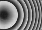
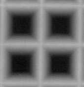
HEBS-glass masks having gray levels ranging from 16 to many hundreds were fabricated via e-beam direct write in HEBS-glass. For example, a very high quality, sinusoidal absorption grating 2cm × 2cm in size having 625 gray levels within each period of 250µm ± 0.2µm was fabricated using Cambridge EBMF 10.5 e-beam writer. The grating is a series of linear strips, 2cm long whose absorbence varies sinusoidally along the direction perpendicular to the strips. The linear strip which is the lines of constant optical density, has a requirement of better than ± 0.1µm in linearity. Within each period, the minimum transmission at the wavelength of 435nm is 1% of the maximum transmission. One each of the gratings satisfying the above specifications was fabricated using the write scheme of Table 1 and the write scheme of Table 2. 625 clock rates were determined from equation 1 for the grating fabricated using the write scheme of Table 1. A different set of 625 clock rates were determined from equation 2 for the grating fabricated using the write parameters of Table 2. The minimum and the maximum optical density values of the 625 gray levels are 0.172 and 2.172 using the write scheme of Table 1, and are 0.178 and 2.178 using the write parameters of Table 2.
Using a gray level mask in an optical exposure system, the throughput of resist exposure in DOE fabrication increases with a lower value of the minimum optical density level in the gray level mask. It is therefore desirable to have the optical density value of the lowest gray level being about or below 0.1. However, using the write parameters of Table 2 and the clock rates of 10 MHz to 0.4 MHz, net optical density values of HEBS-glass upon e-beam exposure range from 0.178 to 2.208. Since 10 MHz is the maximum clock rate available using a Cambridge EBMF 10.5 e-beam writer, to reduce the minimum optical density value below 0.178, it is necessary to decrease the beam current from 75 na, therefore, reducing the throughput of mask making.
A vector scan e-beam writer having the capability of higher clock rates can be employed to increase the throughput of mask making and also to reduce the minimum optical density value toward zero (from 0.178). The capability of focusing a larger beam current to a given e-beam spot size is an important feature to take full advantage of a higher clock rate.
It is known that the sensitivity of HEBS-glass is enhanced by the heat effect of a larger beam current. The throughput of writing a HEBS-glass gray level mask increases by a factor of 7.5 instead of 4 when the addressing grid size is increased from 0.2µm to 0.4µm, and at the same time the beam current is increased from 75na to 300na. To maintain an optical density value of about 0.17 for the lowest gray level, the write scheme of Table 1 has a beam current of 250na instead of 300na. Nevertheless, the throughput of writing a HEBS-glass mask using the write parameters of Table 1 is still 6.25 times the throughput using write parameters of Table 2.