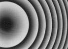
Fabrication of HEBS-glass Gray Level Masks
A HEBS-glass photomask with multi-gray levels is ideally suited for fabrication of diffractive optical elements, refractive micro optics, micro-electro-mechanical devices, micro-opto-electro-mechanical devices and integrated optical components, and for beam shaping optics.
A mask for multi phase levels of DOE is made by exposing in an e-beam writer with predetermined dosages according to calibration curves such as that shown in Fig. 13 and 14 together with that shown in Figs. 7 and 8.
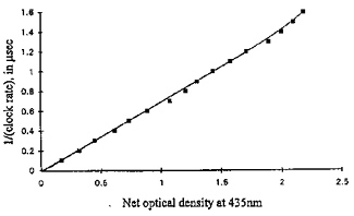
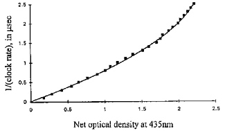
To make a HEBS-glass gray level mask using a vector scan e-beam writer, optical density levels which will achieve evenly spaced multi depth levels over the thickness range of photoresist needed for a subsequent dry etching, are determined from a calibration curve of e.g. Fig. 13 or Fig. 14. Each optical density level in the mask is then written with a clock rate corresponding to the predetermined optical density value. The clock rate is determined from the calibration curve such as that shown in Fig. 15 and Fig. 16. The calculation of the clock rate is further elaborated below.
The clock rates f were calculated from polynomial equations such as eq. 1 and eq. 2 for a large number of the predetermined optical density levels of gray level mask designs. Eq. 1 and eq. 2 are the best polynomial fit equations of the experimental data of Table 1 and Table 2 respectively.
Eq. 1 => 1/f = 0.0478 D4 - 0.1879 D³ + 0.2587 D² + 0.58 D + 0.0021
Eq. 2 => 1/f = 0.1729 D4 - 0.5908 D³ + 0.7685 D² + 0.4592 D + 0.0056
Plotted the experimental data of Table 1 together with equation 1, Fig. 17 exhibits the calibration curve "1/(clock rate) versus net optical density at 435nm" for the e-beam write scheme of 30kv, 250na beam current and 0.4µm addressing grid size.
Plotted the experimental data of Table 2 together with equation 2, Fig. 18 displays the calibration curve "1/(clock rate) versus net optical density at 435nm" for e-beam write scheme of 30kv, 75na beam current and 0.2µm addressing grid size.