Cost Efficient Mass Fabrication of Asymmetric Irregularly Shaped Micro Lens Arrays
A cost-effective way of fabricating large arrays of refractive micro lenses becomes more and more important. Gray level mask fabrication offers the possibility to shape arbitrary resist profiles and therefore produce arrays of general aspheric non-rotationally symmetric refractive lenses with different functionality, complete aberration correction and a 100% fill-factor. The fabrication method based on HEBS-glass gray level mask allows for complete freedom in terms of the shapes e.g. asymmetric, irregularly shaped lenses, and location of the lenses e.g. with accurate center to center spacing.
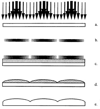
As the resist for the lithography step a comparatively thick photoresist e.g. the Shipley S1650 is employed in order to achieve a resist thickness in the range of 5 to 10 microns. This feature depth in resist will allow for a total lens sag after the etching transfer of about 30 to 50 microns, since a magnification of the feature depth of about a factor of 3 to 5 can be achieved during the transferring step of resist profiles into their respective substrates via Chemically Assisted Ion Beam Etching (CAIBE). The described fabrication steps are shown in Fig. 12.
For the analog transfer scheme of Fig. 12, i.e. from an optical density profile in the gray-level mask into a surface height profile in the photoresist, it is necessary that the number of gray levels be increased as the aperture of the refractive lens increases; for example, HEBS-glass masks having a minimum of 32, 64, and 96 gray levels are needed to fabricate refractive micro lenses having apertures of 50µm, 100µm, and 200µm, respectively.