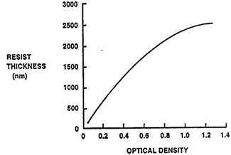
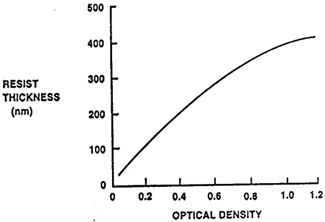
Fig. 13 shows the remaining thickness after development of Shipley S1650 photoresist as a function of the optical density at 436nm of the gray levels in a HEBS-glass mask. The initial (i.e. as coated) thickness of the Shipley S1650 photoresist was 4.0µm Fig. 14 shows the remaining thickness after development of OCG OeBR-514 photoresist as a function of the optical density at 436nm of the HEBS-glass. The initial thickness of OCG OeBR-514 photoresist was 0.8µm. Both calibration curves were done with a vacuum contact aligner.
Fig. 13 together with Fig 14 serves to demonstrate that the range of resist thickness in the depth versus optical density calibration curve can be altered through the choice of a photoresist and/or resist parameters, the initial thickness of the photoresist in particular. In the plots of resist thickness versus optical density, the slope of the calibration curve reduces as the developed resists thickness approaches the initial resist's thickness. Therefore, to produce an analog resist profile of a given feature depth, it is necessary to start with an as coated resist thickness which is more than that of its required feature depth.
To transfer multilevel resist structure of DOE into quartz through a dry etching process, the relative etch rate between photoresist and quartz substrate can be so chosen to achieve the final needed etch depth 3 to 6 times that in the resists. Therefore, for the fabrication of DOE in quartz, a surface height variation of e.g. 350nm in the resist results in a depth modulation in quartz of up to 2100nm.
(b) Optical density versus electron dosage, i.e. a calibration curve of e-beam exposure.
Fig. 7 and Fig. 8 depict the exemplary calibration curves of e-beam exposure. For DOE fabrication, the required optical density values of a HEBS-glass gray level mask are typically in the range of 0.1 to 1.2. Therefore, the required e-beam dosages to obtain optical density values in the ranges of 0 to 1.2 of e.g. Fig. 7 and Fig. 8 constitute the DOE calibration curve of e-beam exposure.
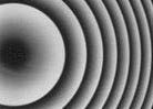
For the fabrication of refractive micro lens arrays, the optical density levels in a HEBS-glass gray level mask is in general in the range of 0 to more than 1.2. The maximum optical density value is larger to produce a larger lens-sag.