(c) Optical density versus clock rate, i.e. another calibration curve of e-beam exposure.
The electron dosage D in microcoulomb/cm² is calculated as follows:
D(µc/cm²) = I · t · N = I · N/f
Where I is beam current in amp., t is exposure duration i.e. dwell time per pixel in µsec, and N is number of pixels in 1 cm². The exposure duration per pixel is equal to 1/f, where f if the clock rate i.e. the write frequency. Since the clock rate can be varied on the fly using a vector scan e-beam writer, the calibration curve "optical density versus clock rate" is a practical one for a vector scan e-beam writer. The calibration curve was determined experimentally for each combination of write parameters which include beam acceleration voltage, beam current and addressing grid size. For example curve B of fig. 7 was determined as follows:
A HEBS-glass plate, part number N20I85CR5090, was exposed with 30 square areas of 3mm × 3mm using a Cambridge EBMF 10.5 e-beam writer. The e-beam writer was operated at 30kv, 75na beam current and a 0.2µm address size. The exposure duration per pixel was 0.1µsec for the first square area and was 3.0 µsec for the 30th square area. The exposure duration per pixel for each of the square areas, first to 25th square, was listed in Table 2. The corresponding clock rate and electron dosage were also listed in Table 2. Net optical density values in the spectral range of 350nm to 700nm were measured using a Hitachi U2000 spectrophotometer. Due to the small sample area of 3mm × 3mm, the net optical density values of the 26th to 30th square areas were too high to be measured as accurately as the rest of the e-beam darkened square areas and were not listed in Table 2. The measured net optical density values at 435nm, 530nm, and 630nm of the e-beam darkened square areas were exhibited as curve B in Fig. 7(a), Fig 7(b) and Fig. 7(c) respectively and were also listed in Table 2.
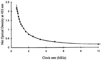
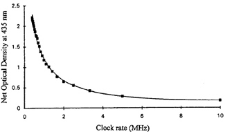
The net optical density values at 435nm and the corresponding clock rates are plotted in Fig. 15 and Fig. 16, using the data points listed in Table 1 and Table 2 respectively. Fig. 15 exhibits the calibration curve "net optical density versus clock rate" for the e-beam write scheme of 30kv, 250na beam current and 0.4µm addressing grid size. Fig 16 displays the calibration curve "net optical density versus clock rate" for the e-beam write scheme of 30kv, 75na beam current and 0.2µm addressing grid size.