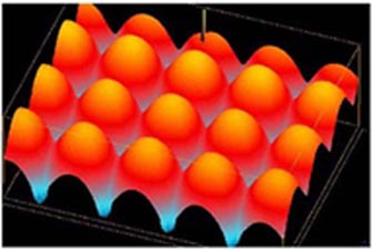
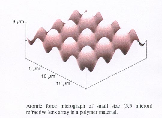
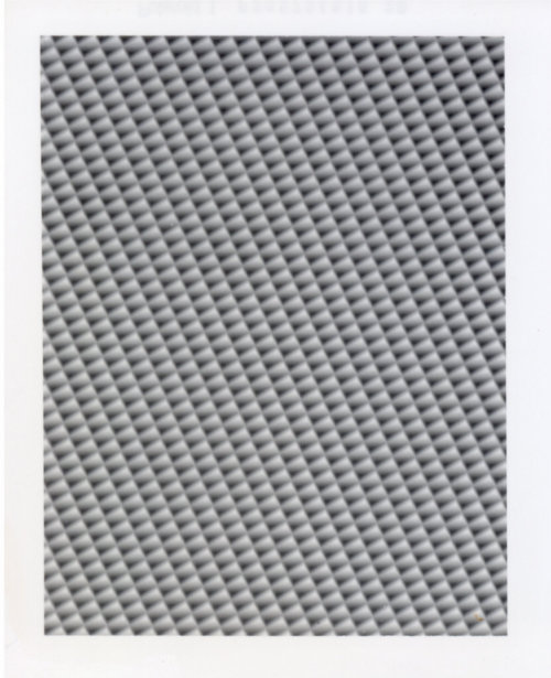
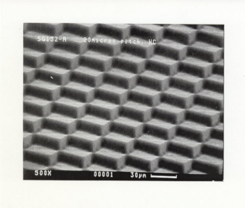
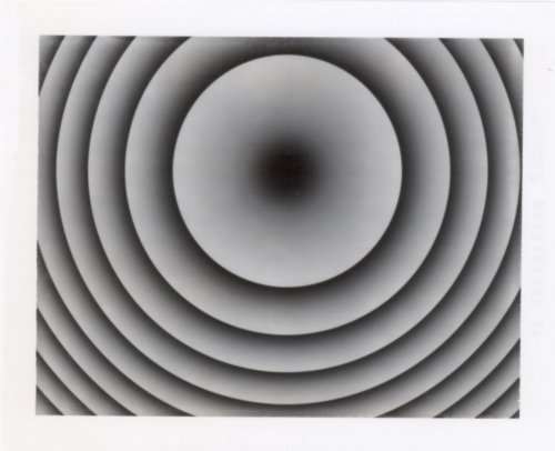
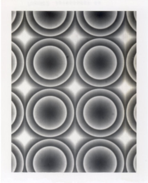
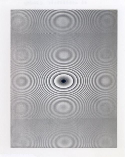
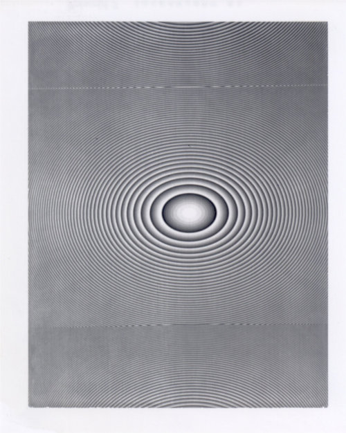
Photosculpting the photoresist (or other photosensitive materials) by spatially variable exposure.
When a true gray scale mask is used to print on photoresist, a different transmittance value in the mask results in a correspondingly different thickness or height in photoresist. Namely, the thickness of the photoresist after development depends on the local dose of UV irradiation.
Local dose is adjusted by the mask transmittance which may also take into account the non-linear photoresponse of the particular photoresist and proximity effects.
Having no coating of any kind, there exist no scattering from line edges; as a consequence, a gray scale optical density pattern in a mask is faithfully and reproducibly converted into a designed gray scale height profile in photoresist using a conventional uv exposure tool.
The development time and conditions are controlled to achieve the desired "analog" photoresist profile.
All-glass gray scale photomasks enable economic mass fabrication of high quality micro-optical elements using a conventional UV exposure tool.
All-glass Gray Scale Mask Technology broadens the reange of applications of photoresist-based refractive and diffractive micro-optics fabrication.
All-glass Gray Scale Mask Technology enables the fabrication of precision and arbitrary shaped micro-optics and other 3D microstructures (including optical MEMS).
All-glass Gray Scale Mask Technology enables reproducible fabrication of each lenslet in a microlens array to better than one tenth of a wavelength accuracy.
Even for the fabrication of only a single mold surface for compression molding or embossing of plastic optical elements, photolithography using an all-glass gray scale mask is the preferred choice over laser beam direct write or e-beam direct write on photoresist.
The advantages of photolithography using an all-glass mask over direct write on photoresist include:
1. An all-glass gray scale mask enables economic optimization of development time and conditions of photoresist process to obtain the most desired analog resist profile in the presence of many variable parameters, such as type of resist, as-coated resist thickness, resist processing variables, and uv exposure variables.
Without the mask to optimize the above listed variable parameters, numerous repeats of direct writing on photoresist are needed.
2. 3D microstructures in photoresist of up to and beyond 20 microns deep can be fabricated because a gray scale mask is used in a conventional UV exposure tool that uses a collimated beam. Whereas a limit on the depth of the structure exists for electron beam as well as laser beam direct write on resist.
3. Due to spot size of laser beam, there is limit on shape accuracy and roughness for laser direct write on photoresist. This limitation is circumvened by using an LDW mask. Due to heat erasure mode of recording and heat threshold effect of LDW glasses, the recorded spot size in LDW glass is submicron even when the laser focused spot size is substantially more than 1 micron.
4. Polymer master mold (e.g. poly-urethene acrylate mold) is made using an all glass gray scale mask without the problems of mold deformation by heat during e-beam or laser beam direct write.
5. Other merrits of the all-glass gray scale mask technology include:
5a. simple lithographic process enables economic mass production in high quality of micro optical elements;
5b. high spatial and grayscale resolution which are needed to produce exact surface profiles;
5c. a gray level width may be 0.1 micromter in the all glass mask, and the resolution can be further enhanced by use of a reduction stepper;
5d. unlike halftone masks such as chrome masks that rely on varying pinhole density, LDW-glass and HEBS-glass masks are the true gray scale photomasks that enables reproducible and faithful conversion of gray scale optical density levels in a mask into corresponding gray scale height levels in photoresist;
5e. predetermined gray levels are obtained by beam exposure of a surface glass layer to a range of dosage (beam current x dwell time);
5f. there is no coating of any kind and no post exposure processing of any kind that increases the cost and defects such as pinhole density;
5g. conventional contact aligners and projection printers and reduction steppers are used without any special requirements;
5h. continuous optical density values of up to 1000 levels can be obtained within an OD range of 0 to 2.0.


